Computer Architecture
These are notes for the version of the class which is being taught by professor Naghmeh Karimi in the Spring of 2016.
-
Textbook: D.A. Patterson and J.L. Hennessy, Computer Organization and Design: The Hardware/Software Interface - 5th edition
-
Grading:
- Homework and Quizzes: 30%
- Midterm: 30%
- Final: 40%
Course Goals
- Ability to define the principles of Computer Architecture
- Ability to write assembly programs
- In-depth understanding of integer and floating point architectural blocks
- In-depth understanding of the datapath inside a processor
- In-depth understanding of pipelining for 32-bit architectures and pipeline hazards
- Ability to understand and analyze computer memory hierarchy
- Ability to understand computer busses and input/output peripherals
Lecture Topics
- Intro, History of Computers
- Assembly Instructions
- Processors (datapath and controller)
- Memory Hierarchy
- I/O devices
- Multi-core
Lecture 1 - Introduction
1958: First integrated circuit
- Flip-flop using two transistors @ Texas Instruments
In 50 years we went from 2 transistors to 55 million! This was driven by the miniaturization of transistors.
Computers have been increasing in speed and decreasing in size (really the transistors have!) since their inception in the 1950’s and 60’s
It has been followed by Gordon Moore’s Law (more commonly known as Moore’s Law) that the amount of transistors that could fit on a silicon die would double every 2 years. Surprisingly his law holds true almost all the way from the 1960s when he first predicted this, all the way until now (2014/2015)!
However one downside to this is that the power consumption of these chips has been increasing as well.
Lecture 2 - Introduction 2
We want to look at how these computers are structured and organized though. What exactly does it do?
- Instruction set, registers
- MIPS, x86, Alpha, PIC, ARM
- Microarchitecture
- Single cycle, multi-cycle, pipelined, superscalar?
- Logic: how are functional blocks constructed?
- Ripple carry, carry look-ahead, carry select adders
- Circuit: how are transistors used?
- Complementary CMOS, pass transistors, domino
- Physical
- Chip layout
There are different classes of computers which we should consider.
- Desktop Computers
- Designed to deliver good performance for a single user at a low cost. Typically use mouse and keyboard
- Servers
- Used to run larger programs for multiple simultaneous users typically accessed only via a network and that places a greater emphasis on dependability and often security
- Supercomputers
- A high performance, high cost class of servers with hundreds to thousands of processors, terabytes of memory and petabytes of storage that are used for high-end scientific and engineering applications
- Embedded Computers (Procesors)
- A computer inside another device used for running one predetermined application
What happens below a program in a computer?
Usually it’s written in a high-level language which was translated (compiled) from the programming language to machine code. From there the operating system is able to take the machine code and turn the machine code to service code which handles the input and output, memory management and storage, and scheduling tasks and sharing resources.
All of these instructions are then sent to the Hardware (processor, memory, I/O controllers).
Most of this information in a computer is all translated into different languages. Usually you start at a High-Level language (c/java), it is then turned into assembly language, a textual representation of instructions for I/O and arithmetic, etc.. Assembly is then translated into binary bits (1’s and 0’s).
An assembler is analagous to a compiler in that it translates the assembly language into binary machine languages.
Computers are really just large abstractions of many different components of a computer. I/O components
- Controllers need to have:
- Ability to input instructions from memory
- logic and means to control instruction sequencing
- logic and means to issue signals that control the way information flows between datapath components
- Logic and means to control which operations are performed
- Datapath needs to have:
- Components - functional units (e.g. adder) and storage locations (e.g. register file) - are needed to execute instructions
- Components interconnected so that the instructions can be accomplished
- Ability to load data from and store data into memory
- Processors fetch instructions from memory
- The controller decodes the instruction to determine what to execute
- Datapath will then execute the intruction as directed by the controller
- Upon completion the data output will be stored in memory
- The output device will then output the data
But what exactly is the interface between the software and the hardware?
It is the instruction set
Instruction Set Architecture (ISA)
- It is the actual programmer-visible instruction set
- Boundary between software and hardware
- Decisions regarding
- Class of ISA
- Register memory ISA (memory can be accessed by many different instructions)
- Load-store ISA (only load/store instructions can access memory)
- Memory addressing (byte addressable)
- Addressing modes (register, immediate, displacement, …)
- Instruction operands (size/type)
- Operations (data transfer, arithmetic/logical, control, floating point)
- Control flow instructions (connditiona/uncondfitional branches, call/return)
- Instruction encoding (fixed/variable length)
- Class of ISA
Lecture 3 - January 26th 2016
Most of the time when we think performance we think “execution time” or “response time”. For a computing system, or processor. There are many factors of the processor design which can affect the time it takes to a execute a specific program.
Generally the response time is proportional to the clock speed and instructions per clock cycle.
Maximizing performance means minimizing execution time.
We can give a general comparison of the speed of two processors running the same program by using the following equations.
\[\frac{Performance_x}{Performance_y} = \frac{Time_x}{Time_y}\]
Example: if A runs a program in 10 seconds and B runs the same program in 15 seconds, then A is 1.5 times faster than B.
In measuring the exact time it takes to run a program, we can take a very basic understanding that we can run x number of instructions per cycle, how many instructions we need for a whole program to run, and finally the number of seconds for a single clock cycle.
This will give us that program run time is:
\[\text{CPU Time} = \frac{\text{Clock Cycles}}{\text{per Instruction}}\times\text{# of Instructions}\times\frac{Time}{\text{per clock cycle}}\]
One important thing to note with this abstraction is that we assume every instruction takes the same amount of time. This is necessarily always true. Generally a load or retrieval from memory will take a longer amount of time
Lecture 4 - January 29th 2016
Assembly Language
Assembly is the language of the machine. It’s primitive and has no real sophisticated control flow. Instructions are also very restrictive with what exactly you can do.
During this course we’ll work with the MIPS instruction set
- It’s similar to other architectures developed since the 1980’s.
- Used by NEc, Nintendo, Silicon Graphics, Sony, etc..
- 32-bit architecture
- 32 bit address line
- data and addresses are 32 bit
The Instruction Set is the repertoire of instructions that a computer has the ability to use. Different computers will have different instruction sets (bt many aspects will be in common!)
Early computers had simple instruction sets. Now they can be much more complex. But simple ones do still exist!
RISC Philosophy
- Fixed Instruction length
- load-store instruction sets
- limited number of addressing modes
- limited numer of operations
Examples:
- MIPS, Sun SPARC, HP PA-RISC, IBM PowerPC, …
CISC (C is for Complex!). Ex: Intel x86, AMD64
MIPS (RISC) Design Principles
- Simplicity Favors regularity
- Opcode is always the first 6 bits
- Smaller is faster
- limited number of registers
- limited number of addressing modes
- Make the common case fast
- arithmetic operands from register file (load-store)
- Allow instruction to contain immediate operands
- Good design demands good compromises
- 3 instruction formats
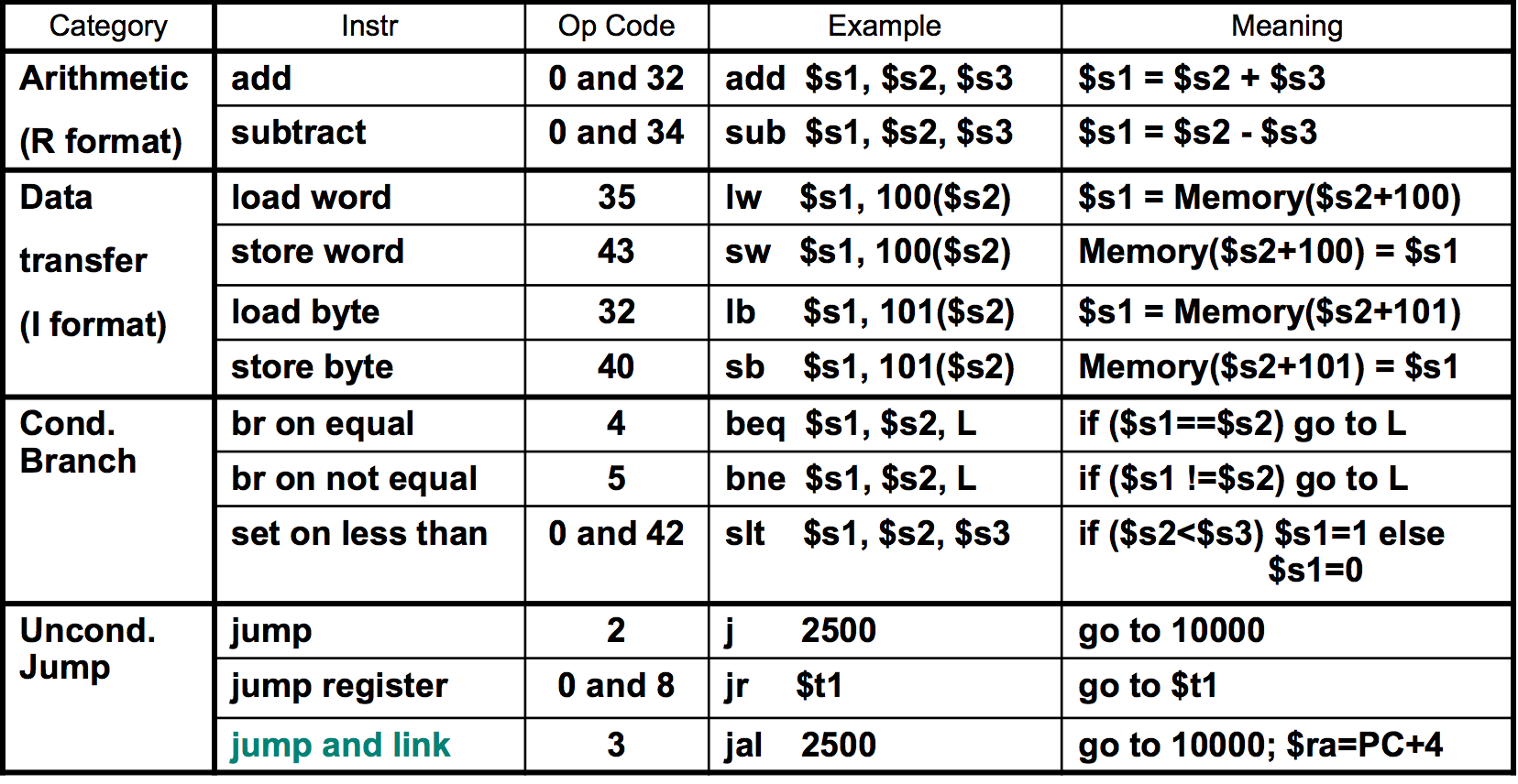
There are 6 different instruction categories for MIPS-32 ISA
- Computational
- Load-Store
- Jump and Branch
- Floating Point
- Memory Management
- Special
Registers are places where we can store values for variables in assembly
There are many different registers in MIPS. The register $r0 always contains the value 0. We also have registers 0-31, HI, LO, and the PC (program counter)
There are 3 types of instruction formats which are all 32 Bits wide
R Format
| op | rs | rt | rd | sa | funct |
I Format
| op | rs | rt | immediate |
J Format
| op | jump target |
MIPS R-Format Instructions
| op | rs | rt | rd | sa | funct |
| 6 bits | 5 bits | 5 bits | 5 bits | 5 bits | 6 bits |
Instruction fields:
- op - operation code
- rs - first source register
- rt - second source register
- rd - destination register
- shamt - shift amount
- funct - function code
Example C-to-MIPS code:
C Code
f = (g + h) - (i + j);
Compiled MIPS Code
add $t0, $s1, $s2
add $t1, $s3, $s4
sub $s0, $t0, $t1
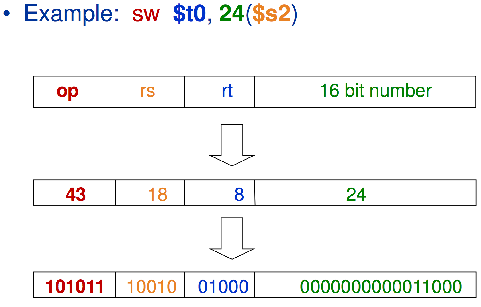
So then how exactly do we translate these statements into binary (1’s and 0’s) that our processor can understand
Recall that R-Format instructions have the format
| op | rs | rt | rd | sa | funct |
| 6 bits | 5 bits | 5 bits | 5 bits | 5 bits | 6 bits |
What if we have the instruction:
add $t0, $s1, $s2
We’ll translate it like this
| op | rs | rt | rd | sa | funct |
|---|---|---|---|---|---|
| special | $s1 | $s2 | $t0 | 0 | add |
| 0 | 17 | 18 | 8 | 0 | 32 |
| 000000 | 10001 | 10010 | 01000 | 00000 | 100000 |
Our final instruction will then be:
00000010001100100100000000100000
Lecture 5 - February 2nd 2016
From here we can actually translate these binary instructions into hexadecimal! The conversion is quite easy using the table below:
| 0 | 0000 | 4 | 0100 | 8 | 1000 | c | 1100 |
| 1 | 0001 | 5 | 0101 | 9 | 1001 | d | 1101 |
| 2 | 0010 | 6 | 0110 | a | 1010 | e | 1110 |
| 3 | 0011 | 7 | 0111 | b | 1011 | f | 1111 |
From this we can translate a binary instruction to hexadecimal:
1110 1100 1010 1000 0110 0100 0010 0000 —> eca8 6420
MIPS Register File
Operands of arithmetic instructions must be from a limited number of special locations contained in the datapath’s register file
The register file holds thirty-two 32-bit registers
This file holds two read ports, and one write port.
Registers are:
- Faster than main memory
- Can hold variables so that code density improves (since register are named with fewer bits than a memory location)
- Register addresses are indicated by using
$.
MIPS Naming Conventions for Registers

Memory Operands
In MIPS all arithmetic instructions’ operands must be loaded into a register before being operated on.
What if a program includes many, many variables (more than you can use in MIPS)?
- Then we must store variables in memory!
- Load values from memory into registers before use
- Store result from register to memory
Memory is byte-addressed, meaning that each address identifies an 8-bit byte.
Words in memory are aligned. Aligned means that the address is a multiple of 4.
MIPS is what we call Big Endian. This means that memory is addressed from left to right, where the beginning of a word is the leftmost position. So in a 4-byte word, the 0th byte is on the left, and the 3rd indexed position is at the rightmost position.
Registers vs. Memory
- Registers are much faster to access than memory
- Operating on memory data requires many loads and stores
- The compiler must use register for variables as much as possible
- Only spill to memory for less frequently used variables.
Accessing Memory with MIPS
MIPS has two basic data transfer instruction for accessing memory
- The data transfer instructions must specify:
- Where in memory to read (load) from or to write (store) - memory address
- Where in the register file to write to (load) or read from (store) (register destination)
-
The memory address (a 32 bit address) is formed by adding the offset (plus or minues) the contents of the base address register.
- A 16-bit field (offset) meaning access is limited to memory locations within a region of \(\pm 2^{13}\) words (\(\pm 2^{15}\) bytes) of the address in the base register.
Processor - Memory Interconnections
- Memory can be viewed as a large, single-dimension array, with an address.
- A memory address s an index into the array.
Accessing memory with lw and sw.
Now imagine we have the C-code:
g = h + A[8];
Imagine g is in $s1, h is in $s2, the base Address of A is in $s3
So because MIPS is addresses words in multiples of 4, then to find the 8th index of the Array, A, with base address 8 * 4 = 32. Meaning that to load the value A[8] we would use the MIPS line:
lw $t0, 32($s3) # Load word A[8] into memory
Then to complete the code translation for this we have:
lw $t0, 32($s3) # Load word A[8] into memory
add $s1, $s2, $t0
Now what happens if instead of 8 as our Array location, we wish to address the array’s index as a variable, say i.
In this case, one option is to multiply the variable by 4, then add that value to the Array’s base address.
From there we may load the variable.
Example. Assume that the base address of Array A is $s3 and that the variable i is represented by $s1.
Then to multiple $s1 by 4 we can do a bitwise shift to the left for 2 bits.
sll $s1, $s1, 2
Then we must add to that the base address of the array
add $s4, $s3, $s1
After which we can then access the memory via
lw $t1, 0($s4)
Lecture 6 - February 5th, 2015
MIPS I format Instructions
| op | rs | rt | constant or address |
| 6 bits | 5 bits | 5 bits | 16 bits |
These I-type instructions allow for ‘immediate’ load and store instructions to the register.
$rtis the destination register- constant is a value between \(-2^{15}\) to \(2^{15} - 1\)
- Address: offset which is added to the base in
$rs
In these types of commands, a constant is specified in the instructions.
For subtraction, we can actually just use a negative constant. So instead of using subi, you can use addi and make the constant negative.
The Constant Zero
The MIPS register 0, ($zero) is always equal to the constant 0. It cannot be overwritten.
It is useful for common operations such as moving between registers
add $t2, $s1, $zero
Loading and Storing Larger (32-bit) Numbers
Due to the format of I-format instructions, it seems such that we cannot immediately load values which are larger than 16 bits into the register. This seems like a limitation, however there is actually a MIPS command which can work around this. It is called lui or load upper immediate.
This stores the largest 16 bits into the register specified with the lui command. You must then use the command ori to store the lower 16 bits into the register, Otherwise just executing the lui will fill the lower 16 bits with 0.
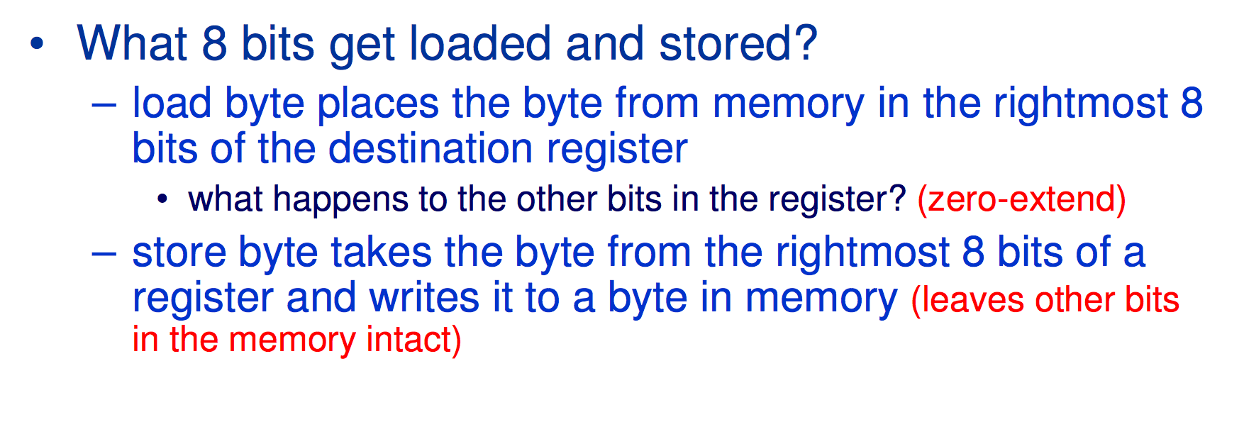
Loading and Storing Bytes
- MIPS provides special instructions to move bytes from memory.
lb $t0, 1($s3) #load byte from memory
sb $t0, 6($s3) #store byte to memory
Logical Operators
| Operation | C | Java | MIPS |
| Shift Left | << |
<< |
sll |
| Shift Right | >> |
>> |
srl |
| Bitwise AND | & |
& |
and, andi |
| Bitwise OR | | |
| |
or, ori |
| Bitwise NOT | ~ |
~ |
nor |
These commands are all useful for extracting and inserting bits within a word.
Shift Operations
These are “R Format” instructions.
They have the form:
| op | rs | rt | rd | shamt | funct |
| 6 bits | 5 bits | 5 bits | 5 bits | 5 bits | 6 bits |
The shift left and right operators (sll, srl)
Lecture 7 - February 9th, 2016
AND Operations
These are useful to mask bits in a word. We can select some bits, or clear others to 0.
Example:
and $t0, $t1, $t2
There’s also an i-format instruction as well
andi $t0, $t1, 0xFF00
OR Operations
The are useful to include more bits in a word. It uses a logical OR to determine whether a bit should be included in the result
There are two form (R and I format):
or $t0, $t1, $t2
ori $t0, $t1, 0xFF00
AND and OR instructions literally check bit by from each word and determine whether the bits should be flipped or not.
NOT Operations
There’s actually no not operator that you can execute against a register
However, it is possible to use a NOR operator
a NOR b == NOT (a OR b)
nor $t0, $t1, $zero
This will flip each bit to the opposite of what is currently in the word
Conditional (Control FLow) Operations
In these instructions we will branch (jump) to a labeled instruction or location if a condition is true
We have 3 different types of control flow operations.
- Branch if equal
- Branch if not eqal
- jump to
Examples of these three instruction (you should be able to figure out which correspond to which)
beq rs rt L1
bne rs rt L1
j L1
L1 is simply a location where we determine j
Compiling IF Statements
In C code we might have something like…
if(i == j)
  f = g + h;
Compiled to MIPS we might see something like:
  bne $s3, $s4, Else
  add $s0, $s1, $s2
  j Exit
Else: sub $s0, $s1, $s2
Exit: ...
Compiling Loop Statements
In C, we might have code which looks something like:
while (save[i] == k)
  i += 1;
Then, if compiled to MIPS using the control statements it will look something like:
Loop: sll $t1, $23, 2
      add $t1, $t1, $s6
      lw  $t0, 0($t1)
      bne $t0, $s5, Exit
      addi $s3, $s3, 1
      j Loop
Exit: ...
Conditional Branches
Instructions:
bne $s0, $s1, Labelbeq $s0, $s1, Label
These I format instructions have the form
| op | rs | rt | jump location |
| 6 bits | 5 bits | 5 bits | 16 bits |
but how exactly is the 16 bit branch location calculated?
Specifying Branch Destinations
Use a register added to the 16 bit offset.
- We will use the instruction address register.
- the PC gets updated during the fetch cycle cso that it holds the address of the next instruction
- This limits the branch distance of an instruction to be \(-2^{15}\) or \(2^{15} - 1\)
Other Conditional Operations
slt rd, rs, rt
- Set result to 1 if a condition is true, otherwise set 0
if (rs < rt), rd = 1;, else rd = 0
slti, rt, rs, constant
if (rs < constant) rt = 1; else rt = 0;
These two can be used in combination with beq and bne
Example:
slt $t1, $s1, $s2 # If ($s1 < $s2)
bne $t0, $zero, L # Branch to L
Lecture 6 - February 12th 2016
Branch Instruction Design
Why don’t we have a blt (branch greater then) or bge(branch greater or equal)?
- The reason is that in hardware these types of instructions are physically slower to run than the \(=\) or \(\neq\)
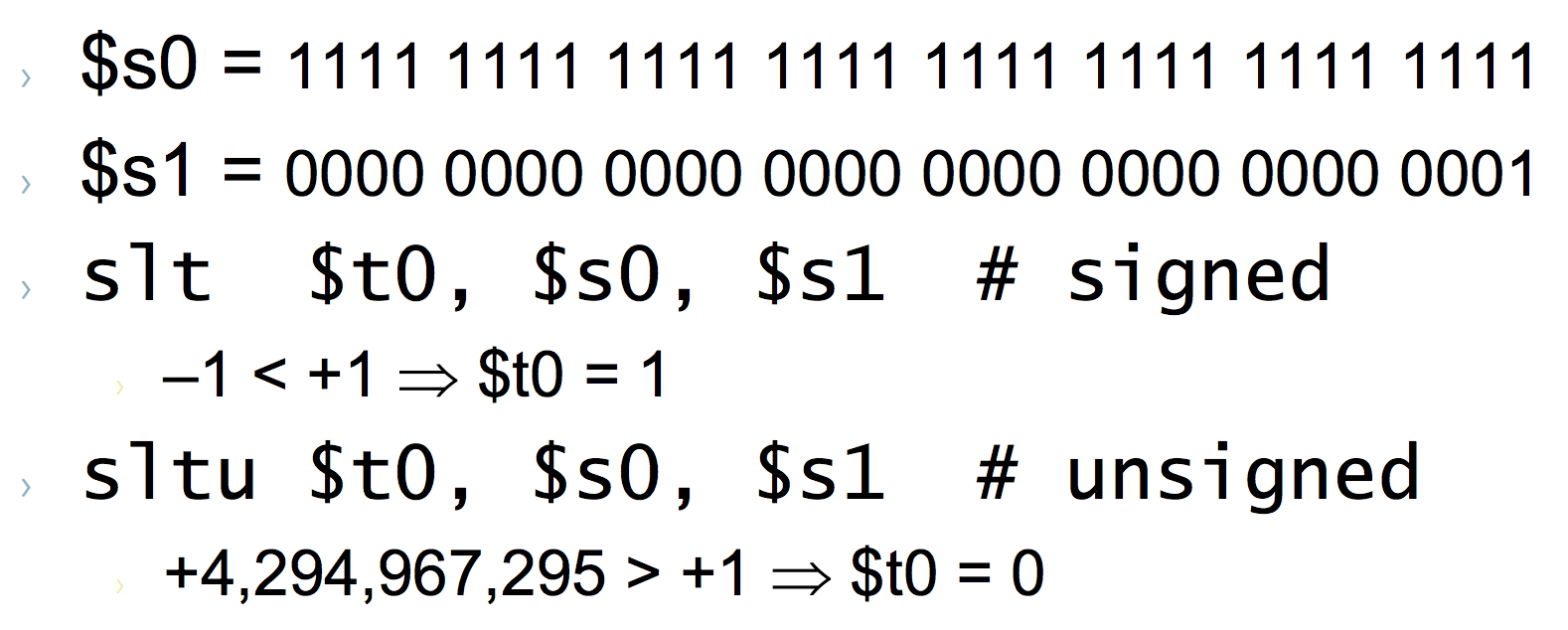
Signed vs. Unsigned
- Signed Comparison instructions:
slt,slti - Unsigned Comparison:
sltu,sltui
Example:
More Branch Instructions
We can use slt, beq, bne and the fixed value of 0 in register $zero to create other conditions
Example: less than
slt $at, $s1, $s2
bne $at, $zero, Label
In MIPS we have pseudo-instructions which allow us to do this on a single line using ble, bgt, bge
Jump Instructions
Just instructions come in the form
j label # Goes to label, 'label'
Machine Format:
| op | 26-bit address |
| 2 | ???? |
But how exactly is the jump destination address specified?
- An absolute address is formed by concatendating the upper 4 bits of the current PC and concatendating
00as the 2 low-order bits.
Branching Farther Away
What happens when a destination address ends up being more than 16 bits away? (the maximum length for a branch location in a bne or beq command.)
The assembler will attempt to then invert the comparison command and then place a j command after the comparison
Example:
beq $s0, $s1, L1
Will then become
  bne $s0, $s1, L2
  j L1
L2:
Procedures
Procedures (also known as methods or functions) in C like languages are usually their own blocks of code which run given a set of arguments.
The issue is that given a procedure we must return to a previous spot in our code form thwere is was originally called. It is possible to do this with assembly.
First let’s look at the main steps of a procedure
- The main routine (caller) places actual parameters in a place where the procedure (callee) can access them.
- Typically registers
$a0 - $$a3
- Typically registers
- The caller transfers control to the callee
- The callee axquires the storage resources needed
- The callee performs the desired task
- The callee places the result value in a place where the caller can access it
$V0and$vare typically the values for return registers
- The callee then returns the control to the caller
$rais the return address register to return to the point of origin.
The format for doing this in MIPS assembly is:
jal procedureAddress # jump and link
This saves PC+4 in the register $ra and then jumps to the address procedureAddress
The callee will then do the procedure return with just
jr $ra
MIPS Register Conventions

Spilling registers
But what will happen if the callee needs to use more registers than allocated to argument and return values?
- The callee will use a stack a LIFO queue
One of the general registers $sp (also known as $29) is used to address the stack which ‘grows’ from high address to low address
- Add data onto the Stack (“push”)
$sp = $sp - 4
- Remove Data from the Stack (“pop”)
$sp = $sp + 4
So what does this mean for us? How can we write a method which uses recursion?
Or in other words **how do we code in assembly, a situation where **
Basically what we need to do is write to (and pull from) the main memory using the stack pointer $sp
We see when using jal and j $ra the PC (Program Counter) is stored to whichever address is currently present in the $sp register.
But if we know that we need to call a recursive function we need to do three separate things:
- Store all of the register values that we need once we get out of the recursive call
- Make the resursive call
- Restore the stack pointer counter to its original position
One thing that should be noted is that the stack pointer starts at high memory addresses and progresses to lower ones
So if we want to save two different register values $t0 and $t1, with our stack $sp, we would write the following
addi $sp, $sp, -12 # Make 3 spaces for our values
sw $ra, 8($sp) # Store return address sp - 4
sw $t0, 4($sp) # Store a variable at sp - 8
sw $t1, 0($sp) # Store a variable at sp - 12
After looking at this code we can see that we first add -12 to our $sp
This creates space for \(\frac{12}{4} = 3\) different register values.
However the original stack pointer $sp should not be modified. This why we store our old $ra with the original stack pointer -4. $sp + 12 - 8 = $ra
Then the same is done for $t0 and $t1
So then what do we do once we get out of the method call? We must return our stored values from the stack
lw $t1, 0($sp) # Put $sp - 12 back to $t1
lw $t0, 4($sp) # Put $sp - 8 back to $t0
lw $ra, 8($sp) # Assign return address original value
addi $sp, $sp, 12 # Return stack pointer to original location
So then if we wanted to generalize the process of performing a method call
- Allocate \(4\cdot(n+1)\) new memory locationd to utilize on the stack pointer where \(n\) is the number of register values that need to be stored. (Use the
addiinstruction) - For each register value which must be stored, use the
swcommand to store each word at a unique$splocation which ranges from$sp- 4(n+1) to$sp- 4 (inclusive). Remember to store the$ravalue! - Then we can call the method using
jal - After returning from the method, restore the register values by using the
lwinstruction to restore the register values from memory. - Continue method execution
Table of MIPS instructions
Byte and Halfword Operations
These instruction can be useful to load values for bitwise operations. In addition to the load byte lb command which will load a single byte from memory, there is also a lh command which stands for Load Halfword which will load only half of a byte.
- Sign extend to 32 bits
lb,lh
- Zero extend to 32 bits
lbu, lhu
- Store just the rightmost byte or halfword
sb,sh
MIPS Addressing Modes
- Register addressing - operand is in a register
- Base (displacement) Addressing - The operand is at the memory location whose address is the sum of a register and a 16-bit constant contained within the instruction
- Immediate Addressing - The oeprand is a 16-bit constant contained within the instruction
- PC Relative Addressing - Instruction address is the sum of the PC and a 16-bit constant contained within the instruction
- Pseudo-direct Addressing - The instruction address is the 26-bit constant contained within the instruction concatenated with the upper 4 bits of the PC
Compilers
A compiler transforms programs from a high level language (like C!) into an assembly language program.
Advantages of high-level languages
- fewer lines of code
- Much much easier to understand and debug
Many compilers today will optimize high-level code and produce efficient assembly code which is nearly as good as an assembly language expert
Assembler
- Transforms symbolic assembler code in object (machine) code
Advantages of assembly language
- Programmer has much more control than higher level languages
- Much easier than remember binary instruction codes
- Can use labels for addresses and let the assembler do arithmetic
- Can use pseudo instructions
However, we must remember tht machine language is the underlying reality
Also considering performance we should still count the instructions executed, not the size of the code.
Other tasks of the Assembler
- Determines the binary addresses corresponding to all labels
- keeps track of the labels used in branches and data transfer instructions in a symbol table
- Converts pseudo-instructions to legal assembly code.
- register
$atis reserved for the assembler to do this.
- register
- Converts branches to far locations into a branch followed by a jump
- Converts instructions with large immediates into a load upper immediate followed by an or immediate
- Converts numbers specified in decimal and hexadecimal into their binary equivalents
- Converts characters into their ASCII equivalents
Memory Layout

Producing an Object Module
- An Assembler (or compiler) translate a program into machine instrucitons.
- It provides information for building a complete program from the pieces.
- Header: described object module content
- Text segment: translated instructions
- Static data segment: data allocated for life of the program
- Relocation info: For contents that depend on absolute location of loaded program
- Symbol table: glocal definitions and external refs
- Debug info: for associating with source code
Linker
- A linker takes all of the independently assembled code and stitches (links) them together
- It is much faster to patch code and recompile and reassemble the patched routine than it is to recompile and reassemble the entire program
- The linker decides on the memory allocation pattern for the code and data modules of each segment
- Remember, segments are assembled in isolation, so each assumes the codes starting and data location are the same.
- Absolute addresses must be relocated to reflect the new starting location of each code and data module
- The linker uses the symbol table information to resolve remaining undefined labels.
Loader
- The loader will load (copy) the executable code which is stored on the disk into memory at the starting address specified by the operating system
- This initializes the machine registers and sets the stack pointer to the first free memory location
- It will copy any parameters to the main routine and onto the stack
- Finally it jumps to a start-up routine that copies the parameters into the argument registers and then calls the main routine of the program with
jal main
Arithmetic With Computers
The first thing that we need to understand is two’s complement.
It is a way of representing positive and negative binary numbers. When we don’t think in two’s complement we typically just think of a number as being the sum of the powers of two in each location where a 1 exists. However, with two’s complement that representation changes.
Take the following example of how to represent the number “-5” in binary with two’s complement
Example: Imagine we have four bits 0000. Say we want to represent the value
-5 using the two’s complement.
- Represent
-5in binary.- \[2^0 + 2^2 = 1 + 4 = 0101\]
- Note
0101, now invert every bit to its opposite value0101inverted1010.
- Add 1 to the inverted value
1010+0001=1011
1011 is the two’s complement representation of the number -5
And what about going backwards (negative to positive)?
Simply subtract 1 from the value, then invert the bits. The exact opposite process from before.
So, to summarize:
To represent a negative number, \(-n\) in two’s complement:
- First represent the number, \(n\), in ‘normal’ binary.
- Invert all of the 1’s and 0’s (turn each 0 to a 1, and each one to a 0).
- Finally, add 1 to the inverted number.
The resulting binary number is now equal to \(-n\)
To find the value of a two’s complement number
- Subtract 1 from the binary number
- Flip all of the ones and zeros
The resulting binary number is the number \(n\) which was represented as \(-n\) in two’s complement.
Two’s Complement Operations
MIPS 16-bit arithmetic gets converted to 32 bit for arithmetic
-
Digits are sign-extended - We copy the most significant bit (the sign bit) into all empty bits
-
Sign extend vs Zero Extend (
lbvslbu)
In sign extension we simply take the rightmost bit of the binary number we’re extending and continuously add that bit (1 or 0) to the left side of the number for however many bits are required.
in zero extension we simply add the required number of 0 bits to the left hand side of the number.
Multiplication with Two’s Complement - Booth’s Algorithm
Given any two numbers which are represented in binary with two’s complement we can multiply them together using Booth’s algorithm (Wikipedia).
The process for multiplying the two numbers are as follows:
Given two numbers to multiply together, say \(m\) and \(n\):
The number of bits in \(m\) is \(x\), the number of bits in \(n\) is \(y\).
The next three terms all have a number of bits equal to \(x + y + 1\)
We can first define a binary number A. Fill the leftmost bits of A with the bits from the number \(m\). The remaining \(y+1\) bits should be filled with zeroes.
Next, we should define the binary number S which is of size \(x + y + 1\). You should fill in leftmost, \(x\) number of bits with the value of \(-m\). In other words: invert the value of \(m\) and then put that binary representation into the leftmost bits of \(S\). The rest should be zeroes
Last, we should define the number P. P is of size \(x + y + 1\) as well. However, we want to fill the most significant (leftmost) \(x\) bits with zeroes. That is The leftmost bits of P should all be zero. The next \(y\) bits should be the value of \(n\). The rightmost bit should be a zero.
Example:
- \[m = 5 = 0101\]
- \[n = 6 = 0110\]
- \[-m = -5 = 1011\]
- \[A = 0101\ 0000\ 0\]
- \[S = 1011\ 0000\ 0\]
- \[P = 0000\ 0110\ 0\]
Now that we’ve defined A, S, and P we can move to the actual algorithm of defining the product of the two numbers. The algorithm is as follows:
- Observe the two rightmost bits of P. Do the following:
- If they are \(01\), set \(P = P + A\)
- If they are \(10\), set \(P = P + S\)
- If they are \(00\), do nothing.
- If they are \(11\), do nothing.
- Do a right bitshift operation on the value of P.
- Make sure that you sign extend when doing this bitshift.
- Repeat steps 1 and 2 until they have been done \(y\) number of times. (\(y\) is the number if bits it takes to represent \(n\))
- The value of the product is the leftmost \(x + y\) bits
Efficient Integer Division with Two’s Complement Numbers
First take two numbers, \(m\) and \(n\). We want to divide \(m\) by the number \(n\).
Next, we need to set up the the quotient/remainder register. Take \(x\) to be the number of bits in \(m\). Zero extend \(m\) so that it is of size \(2x\) bits. This is now the quotient/remainder register.
Remember the divisor is \(n\).
Now for the algorithm:
- Observe the value in the quotient/remainder register. Shift left by 1 bit. (Zero extend from the right hand side).
- Subtract the divisor \(n\) from the left half (leftmost \(x\) bits) of the quotient/remainder register. Remember subtracting is simply adding the negation of the number.
- Observe the leftmost bit of the quotient/remainder register.
- If the leftmost bit is 0, shift the quotient/remainder register left 1 bit, setting the new rightmost bit to 1.
- If the leftmost bit is 1, add the divisor back to the left half of the quotient/remainder register. The value in the left half should now be the same as before step 2. Finally shift the quotient/remainder register left, setting the new rightmost bit equal to 0.
- Repeat steps 2 and 3, up to \(x\) number of times
- Shift the left half of quotient/remainder register right 1 bit.
The division remainder now resides in the leftmost \(x\) bits of the quotient/remainder register. The quotient now resides in the rightmost \(x\) bits of the quotient/remainder register.
Floating Point Representation of Numbers
So we know how to represent positive and negative integers using binary, but what about decimal numbers?
There’s no real ‘intuitive’ way to represent a decimal number using only binary digits, so IEEE made a standard format called IEEE-754 which specifies how to represent postive and negative decimal numbers using 32 binary digits.
The way we represent a floating point number is with the following formula:
\[(-1)^{\text{Sign}} \cdot (1 + \text{Fraction}) \cdot 2^{\text{Exponent} - 127}\]
The question is: What do Sign, Fraction, and Exponent mean in this formula?
Well, IEEE-754 defines a way in which each bit of a 32 bit sequence defined a decimal (or floating point) number.
An IEEE-754 number has the following format
| Sign | Exponent | Fraction |
|---|---|---|
| 1 bit | 8 bits | 23 bits |
As we can see if we add the bits for each space together we get \(1 + 8 + 23 = 32\) bits to represent a floating point number.
Okay, but how exactly do each of these sets of bits help to represent the Sign, Fraction, and Exponent?
Sign Bit
We can see from the above formula that we have \((-1)^\text{Sign}\). What this tells us is that if the sign bit is 0, then the number will be positive because \((-1)^0 = 1\).
On the other hand if the sign bit is 1 then we get \((-1)^1 = -1\) meaning that the number is going to be negative
Exponent
The exponent is interesting. It allows us to represent very, very small numbers as well as large ones using only 8 binary digits.
The exponent values of \(1111\ 1111\) and \(0000\ 0000\) are both reserved for special cases such as Zero, \(\infty\), \(NaN\), etc… They are not used to represent normal numbers. The number we subtract from the exponent (127) is called the bias
Because the exponent is made up of 8 bits that means we can express a maximum of \(2^8 = 256\) numbers (0 through 255). Judging from the formula this means that we can represent everywhere from \(2^{-126}\) (because 0 is reserved, 1-127=-126) to \(2^{127}\) (254 - 127=126, because 255 is reserved).
Fraction
The fraction portion is quite possibly the trickiest of the three to understand. However if we break it down it won’t seem as daunting.
The fraction is represented by the rightmost 23 bits of the floating point number. Each place represents a (negative) power of two. Simply add the powers of two together wherever there is a “1” to calculate the fraction.
Below is a table which outlines the values for the fraction
| 1 | 2 | 3 | 4 | 5 | 6 | 7 | 8 | 9 | 10 | 11 | etc.. |
| \(2^{-1}\) | \(2^{-2}\) | \(2^{-3}\) | \(2^{-4}\) | \(2^{-5}\) | \(2^{-6}\) | \(2^{-7}\) | \(2^{-8}\) | \(2^{-9}\) | \(2^{-10}\) | \(2^{-11}\) | etc… |
Remember that the leftmost fraction bit represents the \(2^{-1}\) place, where the rightmost represents the \(2^{-23}\) place
So if we were given a 23 bit number to represent a fraction, say:
\[1100\ 0000\ 0000\ 0000\ 0000\ 000\]Then the value of the fraction would be:
\[1\cdot 2^{-1} + 1\cdot 2^{-2} + 0\cdot 2^{-3} + 0\cdot 2^{-4} + \dots = 0.75\]Summary
So in quick summary, The formula to represent a floating point number with IEEE-754 standard is:
\[(-1)^{\text{Sign}} \cdot (1 + \text{Fraction}) \cdot 2^{\text{Exponent} - 127}\]The fraction is a sum of negative powers of two, while the exponent field helps represent a power of 2 between \(-126\) and \(+127\). The sign bit simply tells us whether or not the value is positive or negative.
Dealing with Arithmetic Overflow
Some languages (e.g. C) ignore overflow errors.
Some other languages (Ada, or Fortran) will raise an exception.
MIPS handles overflow by attempting to raise an exception. MIPS needs special bits of code called exception handlers to do this.
Using a full single-bit adder we can determine whether there is overflow by looking at the most significant adder (leftmost bit in MIPS).
We must XOR the carry-in and carry-out signals. The result of the XOR will tell us whether there was overflow (1 = true, 0 = false).
| Carry-In | Carry-Out | (Carry-In) XOR (Carry-Out) | Overflow |
| 1 | 1 | 0 | No |
| 1 | 0 | 1 | Yes |
| 0 | 1 | 1 | Yes |
| 0 | 0 | 0 | No |
The Processor
A processor’s clock determines when we can read and write signals. Typically a clock signal will look something like the following:
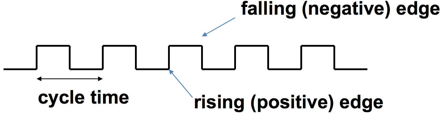
We can see from the image how cycle time is defined. If we wanted the clock rate (frequency) of the clock, then we simply divide 1 by the clock cycle time: \(\text{Frequency} = \frac{1}{\text{Cycle Time}}\)
Elements will perform functions on each rising and falling edge of the clock. Performing operations on each rising and falling edge helps the processor perform more operations in a smaller amount of time.
The Datapath
Instruction Fetch and The PC Register
To execute instructions in a program there are a few different stages. The first is the IF or Instruction Fetch Stage. This stage retrieves the instructions from the instruction memory.
To retrieve instructions from certain locations in memory we use a register called the PC or, Program Counter. This register always holds the byte-address location of the next instruction to be executed.
After one instruction is executed, the PC is immediately incremented by 4, and then passed back for the next instruction (as long as there is no jump or branch statements).
Instruction Decoding
After the instruction is fetched from the instruction memory, it goes onto the next stage of the datapath which is ID or Instruction Decode. The decode stage helps to split up the instruction’s data so that we can read the registers data and certain values are passed to the control unit.
Different intstructions are formatted differently, so we should know the Different formats.
For R-Type instructions, the format is the following
| Bits | 31-26 | 25-21 | 20-16 | 15-11 | 10 - 6 | 5-0 |
| Description | op | rs | rt | rd | shamt | funct |
Load/Store/Branch operations
| Bits | 31-26 | 25-21 | 20-16 | 15-0 |
| Description | op | rs | rt | address offset |
- The difference between the load/store and branch operations is that the address offset of a load/store is for a location in memory, while for the branch instruction it is an instruction memory location.
There’s actually something special going on when executing a branch statement. The new PC value is updated a bit differently than you might think.
Given an unconditional jump instruction, there are 26 bits for the new PC address. To calculate this new PC value, we:
- Sign extend the address to 32 bits.
- Shift this value left two bits (putting \(00\) in rightmost place)
- Concatenate this value to the 4 leftmost bits of the current PC.
This will result in the new PC for the next instruction. However, note that we’re only able to have a maximum jump of \(2^26\)
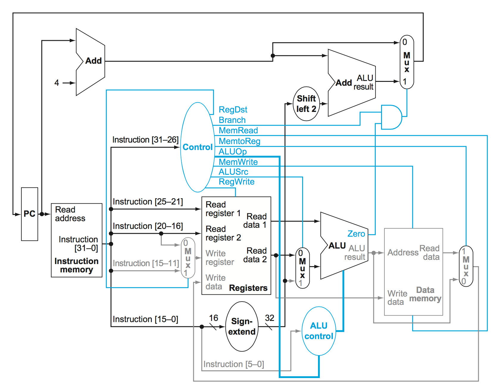
Full MIPS datapath
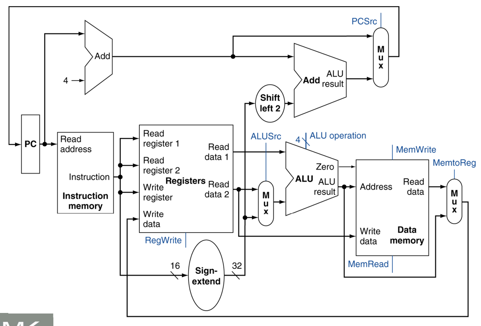
Note the blue lines which go into some of the multiplexers and ALU in this datapath. They specify which data should be selected along certain portions of the datapath
It’s important to note though that no two instructions could “live” inside this datapath at once. We wouldn’t be able to immediately fetch and decode an R-Type instruction after a load/store instruction is fetched/decoded executed, etc.. We would need to wait until the entire load store finished and data was written back into memory (or loaded into a register) before the next instruction could execute.
This is actually very inefficient because this means parts of the datapath end up being unused during the entire process of running an instruction.
Now let’s take a look at the different control lines.
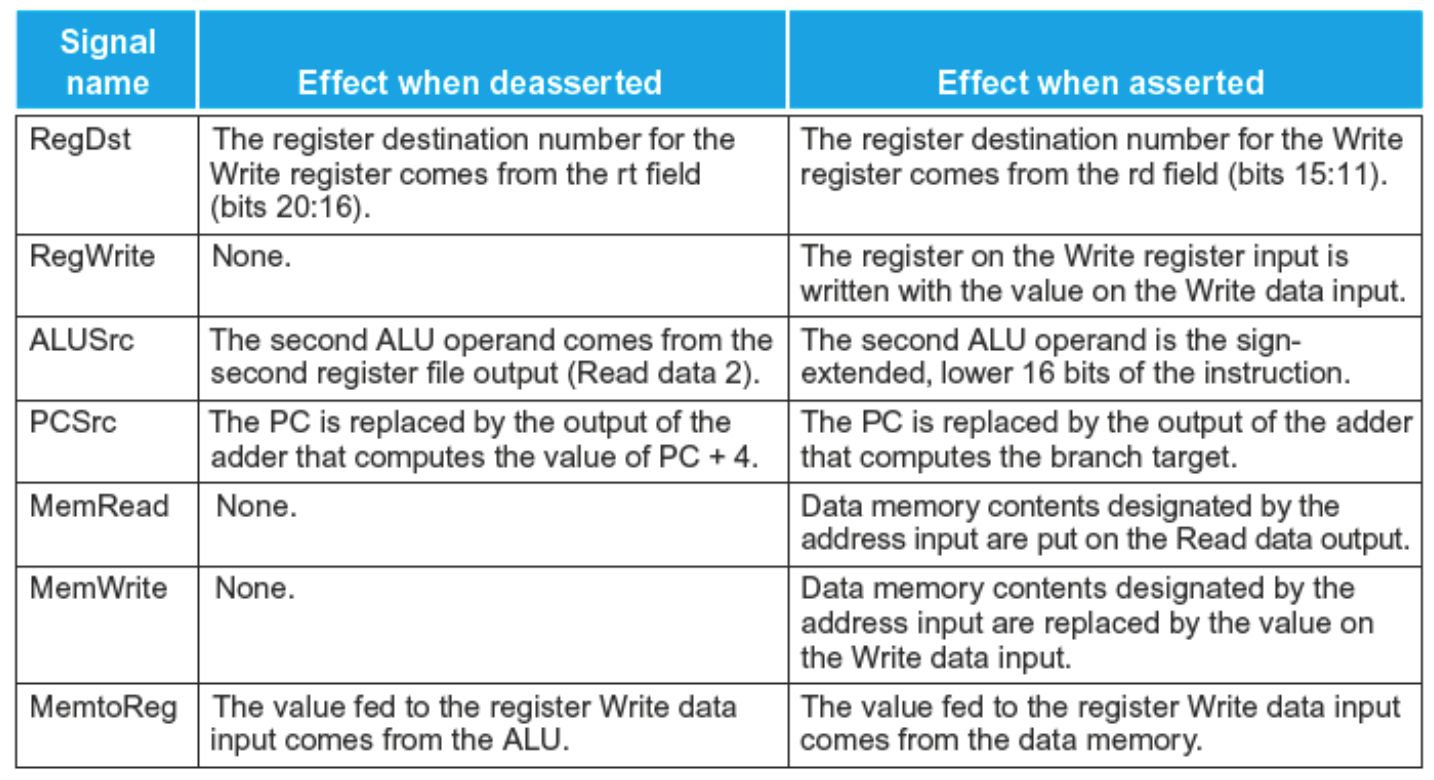
There are actually 8 different control lines. They are:
- RegDst
- Tells whether or not the destination register resides in bits 20:16 (control value 0) or bits 15:11 (control value 1).
- Branch
- Tlles us whether or not an instruction is a branch instruction. AND’d with the zero flag from the ALU
- MemRead
- Tells us whether we need to read from memory or not for the instruction. 1 = true, 0 = false.
- MemtoReg
- Are we moving a piece of data from the memory into a register? 1 = true, 0 = false
- ALUOp
- ALUOp is a 2 bit control which comes from the main control unit. Load/store instructions result in 00. Branch equal instructions have an Opcode of 01. R-types have a code of 10. This code is passed into the ALU control input which uses the Funct field form R type instructions. More on this later.
- MemWrite
- Do we need to write to memory? 1 = true, 0 = false
- ALUSrc
- Does the 2nd operand come from an immediate value? Or is it a register value? 1 - immediate, 0 = register.
- RegWrite
- Do we write to a register with this instruction? 1 = true, 0 = false
Below is a quick table for the instruction bit layout
R-Type
| 31-26 | 25-21 | 20-16 | 15-11 | 10 - 6 | 5-0 |
| op | rs | rt | rd | shamt | funct |
I-Type
| 31-26 | 25-21 | 20-16 | 15-0 |
| op | rs | rt | address offset |
Some observations about these two formats:
- Op field is always bits 26-31
- The registers we always read from are specified by
rsandrtwhich are in bits 16-20 and 21-25. - The address of the register to be written is in two places. Bits place
rtfrom bits 16-20 in lw instructions and thenrdin bits 11-15 for R-type instructions- This explains the RegDst instruction which tells us whether we read from 11-15 or 16-20
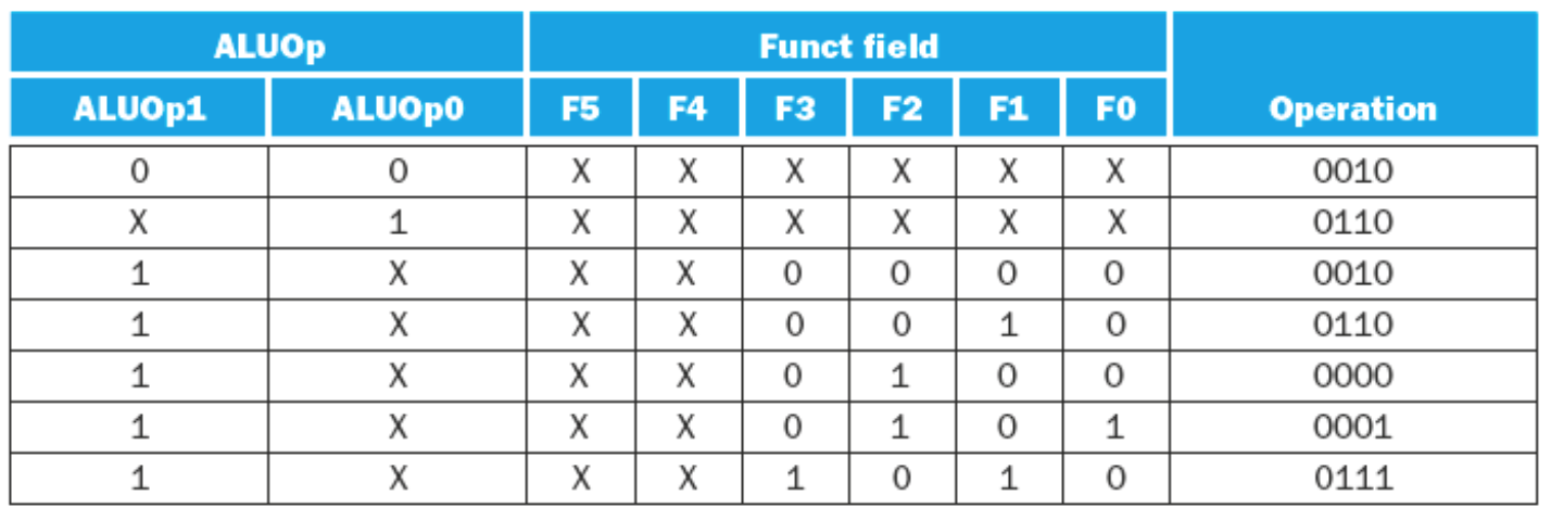
ALU Control Lines
In order to send the right codes to the ALU for the ALU operation the ALU Control must utilize funct bits from the r-type instructions.
The logic for the ALU control is as follows:
- If the ALUOp is 00 (load/store word), then the ALU function is ADD, and the ALU control is the ALUOp +
10\(\rightarrow 0010\) - If the ALUOp is \(01\) then it is a branch equal intruction. The operation should be subtract. The ALU Control is the ALUOp concatenated with \(10\ \rightarrow 0110\)
- If the ALUOp is \(10\) then we need to look at the
functfield from the 0-5 bits of the instruction.- The following table shows the
functfields for typical R-Type instructions -
Operation functAdd \(100000\) Subtract \(100010\) AND \(100100\) OR \(100101\) Set on Less Than \(101010\) - Given each of the
functfields the ALU Control derives the following table of inputs for the ALU
-
Operation functALU Control Lines Add \(100000\) \(0010\) Subtract \(100010\) \(0110\) AND \(100100\) \(0000\) OR \(100101\) \(0001\) Set on Less Than \(101010\) \(0111\)
- The following table shows the
Pipelining with MIPS
The best way to increase performance is with pipelining. It allows multiply instructions to use the datapath at a single time and increases the instruction throughput.
I’m not going to go over all the modifications, but a datapath which supports pipelining is displayed below:
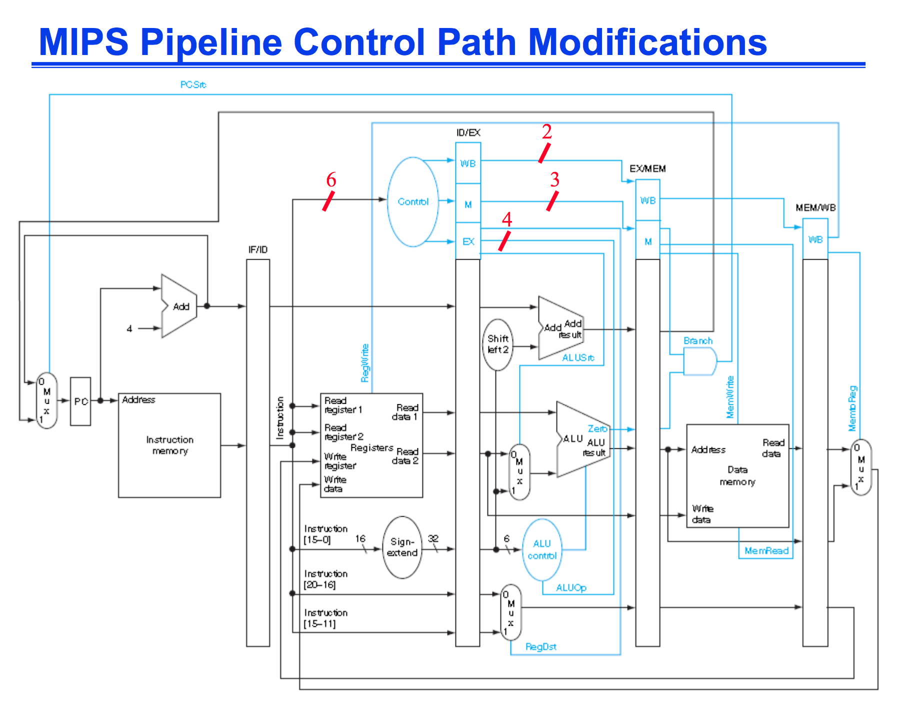
However with Pipelining this introduces something called hazards. Hazards are errors that can possibly occur if we don’t take into account the effects of pipelining.
Example: We load from memory into register R7. We then want to add 5 to R7. In the pipeline, R7 will be loaded at the same time we are adding to R7. But this means we would be adding to the wrong R7 value, so we need to add a stall into the pipeline.
Stalls basically do what they sound like. They stop everything in the pipeline (for one cycle) in order to let the previous operation complete one more stage in order to update for the next instruciton.
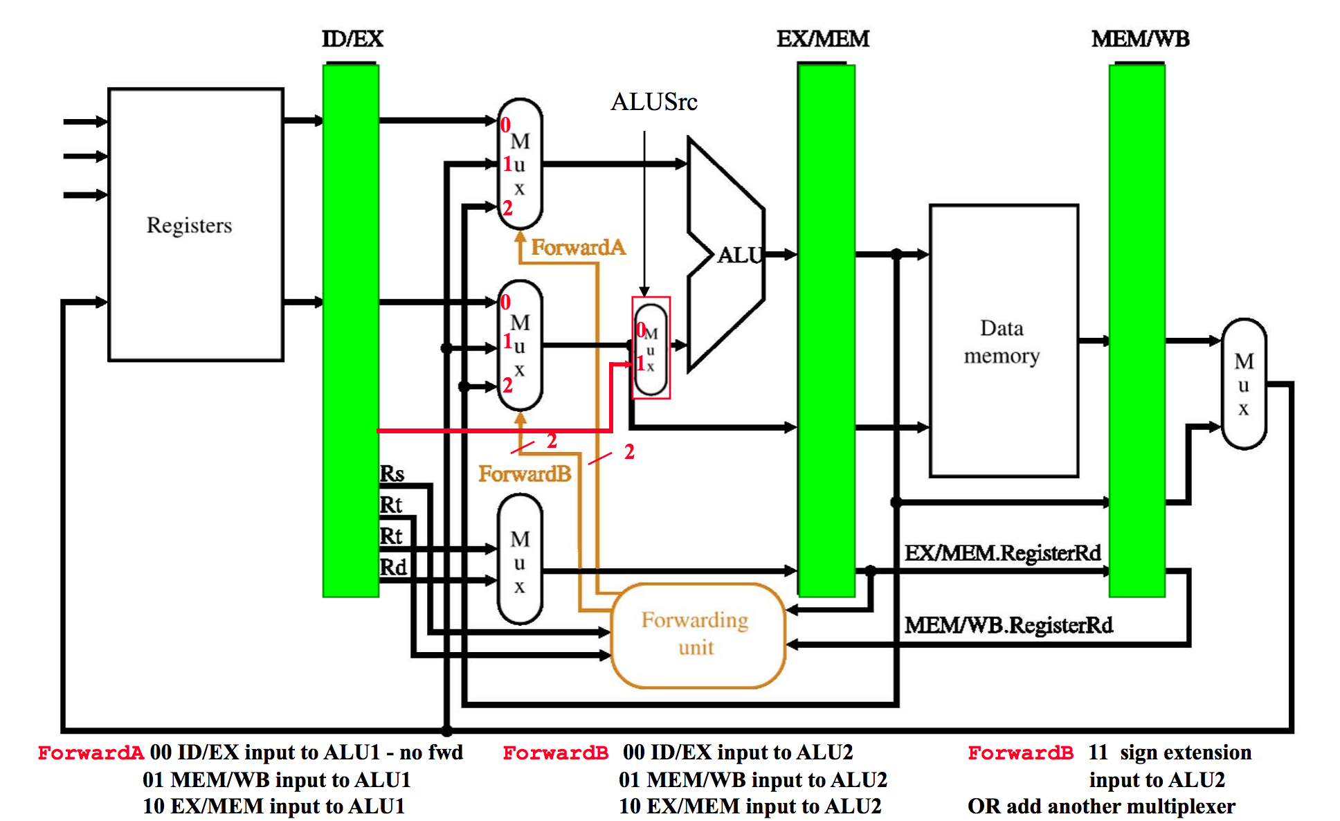
However, we can improve performance even more by introducing instruction forwarding. This reduces the amount of stalls necessary in the processor which makes the datapath even more efficient. We need something called a forwarding unit in order to do this. It sends the data back from certain instructions into the earlier stages to be used with newer instructions.
Memory Heierarchy and the Cache
So typically trying to retrieve data from the memory takes a long amount of time (Hundreds upon Hundreds of clock cycles). If we directly accessed the memory every time we wanted to load a value from the RAM it would cause programs to take a significantly longer amount of time to execute.
So then how do we avoid accessing the memory every single time we execute a lw instruction? We use the cache!
The cache is an intermediary between the main memory and the registers of the processor. Accessing data from the cache is much, much faster than main memory and help our programs run much quicker.
The downside is that faster cache memory is much more expensive than typical DRAM. This is why on even modern processors there are extremely small amounts (compared to DRAM and Hard disk sizes).
Storing Data in the Cache
Because the cache is basically just a much faster, smaller version of main memory, we have to find a method which allows us to map and store different addresses from main memory into the cache.
In this course we will study three main ways of mapping cache locations to main memory.
- Direct Mapping
- Set Associativity
- Full Associativity
A directly mapped cache simply uses the modulus operator on the number of blocks in memory, and then maps it to the cache.
Direct Mapping Example:
- Our memory has up to 10,000 byte locations. Our cache holds 20 blocks (numbered 0-19), storing 1 byte of data in each.
- To directly map a block we simply mod the block address with the number of cache blocks.
- i.e. we want to store memeory block 5454 into the cache, it goes into (\(5454 \% 20 = 14\)) cache block 14.
So we also need to devise a way to tell us whether or not the data in the cache is the data we’re looking for, or if the data in the block is even valid.
We accomplish this using tag and valid bits.
The valid bit tells us whether or not data is event present in the current cache block. 1 = data present, 0 = data not present.
The tag bits are then a set of bits which help identify the the memory location for which the data corresponds to. However, we want to use as few bits as possible to do this. So, the tag for each is actually only composed of the first \(n\) bits of the memory address where
- \[n = \text{bits to address of main memory} - \text{bits to address cache blocks} \\ - \text{bits to address every byte in block}\]
We call the data size for each row of the cache the block size or the size of the data each block of cache is able to hold.
This does not account for the valid or tag bits though.
We should also define hit, miss, hit rate, miss rate, and miss penalty
- Hit: A hit occurs when the data we are searching for appears in some part of the cache.
- Miss: The opposite of a hit. When we are searching for data, but it doesn’t appear in the cache so we must retrieve the data from main memory.
- Hit Rate: The number of times we get a hit divided by the total number of times we attempt to get data from the cache.
- Miss Rate: The number of times we get a miss divided by the total number of times we attempt to get data from the cache.
- Hit Time: The time it takes to determine if the the search for data is a hit or miss + the time it takes to access the cache data.
- Miss Penalty: The time it takes to retrieve from a lower level memory to access a certain piece of data and deliver it to the processor.
Another thing to note is that:
- \[\text{Hit Rate} = 1 - \text{Miss Rate}\]
We can measure cache performance a few different ways:
\[\frac{\text{Memory Accesses}}{\text{Program}} \times \text{Miss Rate} \times\text{Miss Penalty}\] \[\frac{\text{Instructions}}{\text{Program}} \times \frac{\text{Misses}}{\text{Instruction}} \times\text{Miss Penalty}\]There is another metric that is useful to calculate with the cache which is called AMAT, or, Average Memory Access Time.
The formula for AMAT is:
\[\text{AMAT} = \text{Hit Time} + \text{Miss Rate}\times\text{Miss Penalty}\]
So on cache misses and hits we also must devise a strategy to determine how and when we update and interact with the cache and main memory.
Strategies on Cache Hits:
- Write through: Writes to both the cache and memory
- Write Back: Write cache only, memory is updated only when the cache entry is removed
Strategies on Cache Misses:
- No Write Allocate: Only write to the main memory
- Write Allocate: Fetch into cache
The most common combinations are:
- Write through and no write allocate
- Write back with write allocate.
Virtual Memory
Virtual Memory is a concept very similar to the cache, except that typical DRAM is far too small to hold the information necessary to quickly fetch information for many of the programs. Each process running on an operating system will get assigned a range of DRAM addresses to use.
- In other words, main memory (DRAM) acts as a cache for the secondary storage (Hard disk).
- This portion is typically managed by the CPU hardware and the Operating System
-
Each program gets a space in the DRAM to store its data. It is protected from modification by any other programs.
- A virtual memory block is called a page
- A virtual memory translation miss is called a page fault
When a page fault occurs it is millions of clock cycles as a penalty. Typically treated as an exception in the software mechanisms.
The software can help reduce page faults by cleverly deciding which pages to erase or replace in the DRAM.
A write-back mechanism ensures that pages which were altered in RAM are saved to the disk before being discarded. A write-through mechanism is just not practical and takes far too long.
The translation mechanism is provided by what we call a page table.
- Each program has it’s own page table which contains the physical addresses of the pages and is indexed by the virtual page number.
- Because each program/process has its own page table, programs can have the same virtual address space
Reference
MIPS Datapath
Datapath and Control Line Signals
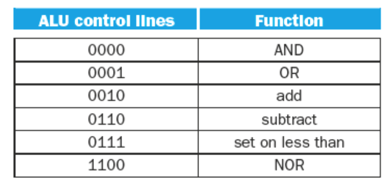
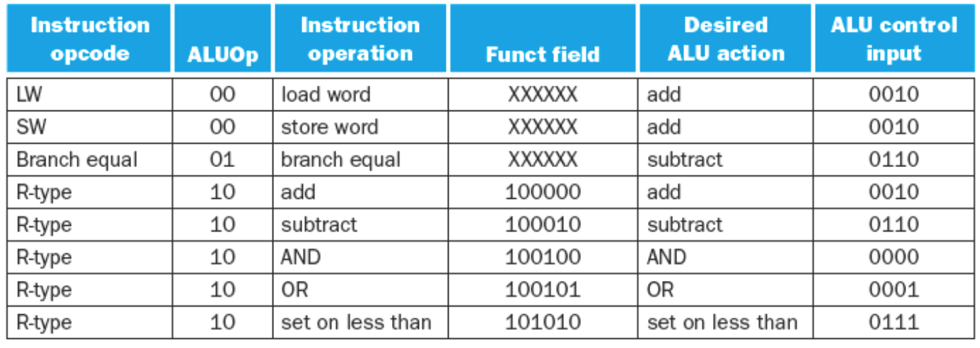
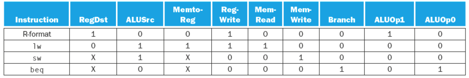
| ALUOp | Action needed by ALU |
| 00 | Addition (for load and store) |
| 01 | Subtraction (for beq) |
| 10 | Determined by funct field (R-type instruction) |
| 11 | Not used |
Pipelined MIPS Datapath