Digital System Design
This was for the version of the class taught in the Fall of 2017
DSD Final Review
Digital System Design is basically a mix of digital logic design and computer architecture put together with a little bit of SystemVerilog mixed in. This page provides the notes I took in order to study for the final exam.
Combinational Logic Design
Combinational logic is defined as having a set of inputs, and a set of desired outputs which can be realized via a timing and functional specification.
A way to think of these circuits is a set of inputs and corresponding outputs for every combination of the inputs where the function is performed by a black box. Inside that black box are the logic gates which define the function and timing performance of your combinational logic.
Product of Sums vs Sum of Products
- Minterm: Product of the inputs
-
Maxterm: Sum of the inverted inputs
- Sum of products is when you sum the minterms together in order to get the logic function
- For every output that is a 1, sum the corresponding minterms
- Product of sums is when you multiply maxterms together in order to determine the logic function
- For every output that is a 0, multiply all of the corresponding maxterms together.
An example is below
Sample function:
| A | B | Y |
| 0 | 0 | 1 |
| 0 | 1 | 0 |
| 1 | 0 | 0 |
| 1 | 1 | 0 |
- SOP: \(Y = \bar{A} \bar{B}\)
- POS: \(Y = (\bar{A} + B)(A + \bar{B})(\bar{A}+\bar{B})\)
Hardware Realization and Function Minimization
Sometimes we can actually implement functions without using the two-level realization from SOP/POS. An example of this is with the XOR function. For a three-input XOR the function is \(Y = ABC + A\bar{B}\bar{C} + \bar{A}B\bar{C} + \bar{A}\bar{B}C\)
Instead of using a two-gate level implementation, you can use a single XOR with three inputs which should be faster than the two-level implementation.
Bubble Pushing
Given a logic circuit we can simplify it with the bubble pushing method.
- Begin at the output, work towards the inputs
- Push any bubbles on the final output back toward the inputs so that you can read an equation in terms of the output (for example, Y) instead of the complement of the output Y’.
- Working backward, draw each gate in a form so that bubbles cancel. If the current gate has an input bubble, draw the preceding gate with an output bubble. If the current gate does not have an input bubble, draw the preceding gate without an output bubble.
This uses Demorgan’s rules where
\[\overline{AB} = \bar{A} + \bar{B}\] \[\overline{A+B} = \bar{A}\bar{B}\]Combinational Timing
- Propagation delay - \(t_{pd}\) - maximum delay from input changing to the FINAL output changing
- This is the typical way we might Contamination delay - \(t_{cd}\) - minimum delay from input changing to when the first output(s) changes before settling on a final value
You can determine the propagation delay by looking at the longest path through the circuit.
Similarly, the contamination delay can be determined visually by looking for the shortest path through the circuit.
Sequential Logic Design
Sequential logic represents the family of digital logic elements which we use to build devices and circuits which are made to work over a period of time where the outputs of the next logic state depend upon the previous outputs. Many of these circuits will contain a CLK signal which controls the frequency at which the device operates.
The main building blocks of sequential logic design are latches and flip-flops.
The most basic latch is the SR Latch which is a pair of cross-coupled NOR gates.
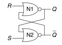
The truth table is as follows:
| S | R | Q | Q’ |
| 0 | 0 | \(Q_{prev}\) | \(Q'_{prev}\) |
| 0 | 1 | 0 | 1 |
| 1 | 0 | 1 | 0 |
| 1 | 1 | 0 | 0 |
Notice the odd behavior of the SR latch when S and R are both asserted. According the the textbook, the SR latch conflates the issue of “what” and “when” which makes understanding this latch sometimes difficult.
The D Latch Solves this issue by using the SR latch and changing its inputs from S and R to D and CLK.
The D latch puts two AND gates in front of the SR latch. The AND before the R input has inputs of CLK and D’. The AND before the S input has inputs of D and CLK.
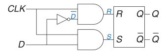
The state table for a D latch is
| CLK | D | Q | Q’ |
| 0 | X | \(Q_{prev}\) | \(Q'_{prev}\) |
| 1 | 0 | 0 | 1 |
| 1 | 1 | 1 | 0 |
Flip Flops
A D flip flop is composed of two D-latches in succession with logically opposite CLK signals. The first latch is connected to D, the Q output of the first latch (master), is connected to the D input of the second latch (slave). This is a flip flop. The purpose of this flip flop is:
- A D flip flop copies the value from D to Q on the rising edge of the CLK and remembers its state at all other times.
A register is simply a bank of flip flops which are all connected to the same CLK signal with different inputs. They allow us to save and output multiple values all at one clock edge.
Enable-able and Reset-able Flip Flops
We can add other inputs to our flip flops by using extra gates outside of them.
You can make a D flip flop enable-able by adding an AND gate in front of the CLK with the ENABLE signal. AND the CLK and ENABLE and you can ensure operation only when the ENABLE is logic high.
You can also make the D flip flop reset-able with the same idea. Use an AND gate in front of the D input. The input to the AND gate is D and RESET’ this way, whenever RESET is asserted, RESET’ is 0 and the result of the AND gate is 0, resulting in the Q ouput being 0 on the next clock edge.
Synchronous Sequential Logic
Synchronous sequential logic is when we have combinational logic where some of the outputs are fed back into the input of the circuit. The catch is that instead of having direct connections, we insert registers in between the output and input. This means the feedback loops change on with the state of the CLK signal. We say that it is synchronized to the clock giving us the name synchronuos sequential logic.
Finite State Machines
- Moore machines the outputs depend only on the current state of the machine.
- Mealy machines the outputs depend on both the current state and the current inputs.
Sequential Logic Timing
For sequential logic to be stable, the outputs must be stable for some aperture time. Similar to how a camera needs the subject to be still for a period of time in order to deliver a crisp picture, a flip flop must have a stable input for a minimum amount of time to be read properly.
Another constraint is that the clock period must be long enough for all signals to settle to their proper values. Overall this limits the speed of operation for an entire system. It is also likely that the clock signal does not reach all elements at the same time. The variation in clock timing is claled clock skew.
The aperture time of a circuit is the sum of the setup and hold time
- \(t_{setup}\) is the time before the rising clock edge that a signal must be stable
- \(t_{hold}\) is the time after the rising clock edge that a signal must be stable
- \(t_{setup} + t_{hold} =\) aperture time
The dynamic discipline of a circuit refers to the fact that the inputs must be stable during the aperture time.
- \(T_c\) is the clock period and represents the time betwen rising edges of the signal.
- \(t_{ccq}\) is the clock-to-q contamination delay. It is the shortest amount of time from a rising clock edge to the Q output changing.
- \(t_{pcq}\) is the clock-to-q propagation delay. It is the amount of time from a rising clock edge to the stable Q output.
Clock time constraint:
\[T_c \geq t_{pcq} + t_{pd} + t_{setup}\]Hold time constraint:
- Basically what this says is that for a register with combinational logic in sequence, the hold time must be less than the clock-to-q and combinational contamination delay in order for the circuit to properly function or else the value of the combinational output will be sampled during unstable periods.
For a circuit without combinational logic, simply having registers/flip-flops in sequence we get
\[t_{hold} \leq t_{ccq}\]Single and multi-cycle timing?
Hardware Description Languages
There are two common prevailing description languages that many logic designers use. VHDL and Verilog. This course mainly just covered using SystemVerilog, an IEEE standard
Everything in verilog is built around hardware modules. You can define the modules with the following syntax
module myfunction(input logic a,
                  input logic b,
                  output logic y);

    assign y = ~a & b | a & ~b ;

endmodule
Simple Combinational Logic
Lots of functions can be expressed as simply a set of gates which don’t have complex functions like sequential synchronous circuits. The functional verilog symbols representing common logic operations are shown below
module myfunction(input logic a,
                  input logic b,
                  output logic y);

    assign y = a & b; // AND
    assign y = a | b; // OR
    assign y = a ^ b; // XOR
    assign y = ~(a & b); // NAND
    assign y = ~(a | b); // NOR
    // Comments can be written with a double-slash '//'

endmodule
Multi-wire blocks
If your circuit has a lot of inputs you can define them kind of like an array where you can access all of the wires via indexing on a single variable instead of having to explicity type all of the variables.
module myfunction(input logic [3:0] a,
                  input logic [3:0] b,
                  output logic y);

    assign y = &a | &b; // AND all of the A's and B's into a single signal, then or the result.
    // Equivalent: y = (a[0] & a[1] & a[2] & a[3]) | (b[0] & b[1] & b[2] & b[3])

endmodule
Conditional Assignments
Like normal programming languages you can write conditional statements to assign values.
module myfunction(input logic a,
                  input logic b,
                  output logic y);

    assign y = a ? a : b;
    // if a == 1, y = a, else assign y = b

endmodule
Adders and Internal Variables
Like normal programming languages you can write conditional statements to assign values.
module fulladder(input logic a, b, cin,
                 output logic s, cout);
    logic p, g;
    assign p = a ^ b;
    assign g = a & b;
    assign s = p ^ cin;
    assign cout = g | (p & cin);
endmodule
Operator Precedence
The following table describes operator precedence in verilog. Note that AND takes precedence over OR
Ordered from highest precedence to lowest.
| Operator | Meaning |
|---|---|
~ |
NOT |
*, /, % |
Mult, Divide, Mod |
+, - |
Plus, Minus |
<<, >> |
Logical Left/Right shift |
<<<, >>> |
Arithmetic Left/Right shift |
<, <=, >, >= |
Relative Comparison Operators |
==, != |
Equality Operators |
&, ~& |
AND, NAND |
^, ~^ |
XOR, XNOR |
|, ~| |
OR, NOR |
?: |
Conditional |
Numbers in Verilog
When writing a number in verilog, the default assumption is that you are writing a decimal number with an arbitary number of bits.
However you can specify how many bits your number is and the base which it is represented (within code). You can do so with the following format.
{#_bits}'{base_type}{number}
I.e. 3b101 represents the number 5 (in decimal) by using 3 bits, 101
Sequential Logic in Verilog
Because a vast majority of logic elements are designed with D flip-flops in modern systems, verilog provides and easy-to-use interface for using these registers to store and update value based on past states.
always @(sensitivity list)
    statement
In this case statement only gets executed if one of the events in the sensitivity list occur. So for a basic D flip flop you could write
module flipflop(input logic clk,
                input logic d,
                output logic q);

    always @(posedge clk)
        q <= d;

    // OR
    // always @(posedge clk)
        // begin
            // q <= d;
        // end

endmodule
you can also use always_ff if your goal is to emulate a flip flop. Verilog tools should throw a warning if you try to use an always_ff statement for anything other than a flip flop. This helps reduce the errors that designers may make when writing the code.
Blocking vs Non-Blocking Assignment
-= is blocking
- occurs one after another
- Mostly used for combinational logic
- Any values which are used after take up the new value
<=is non-blocking- Occurs simulatenously
- Old values are not used.
The general guidelines for blocking and non-blocking assignments are as follows:
-
Use always_ff @(posedge clk) and nonblocking assignments to model synchronous sequential logic.
always_ff @(posedge clk) begin n1 <= d; // nonblocking q <= n1; // nonblocking end -
Use continuous assignments to model simple combinational logic.
assign y=s ? d1 : d0; -
Use always_comb and blocking assignments to model more complicated combinational logic where the always statement is helpful.
always_comb begin p = a ^ b; // blocking g = a & b; // blocking s = p ^ cin; cout = g | (p & cin); end -
Do not make assignments to the same signal in more than one always statement or continuous assignment statement.
Chapter 5 - Adders
The most basic type of adder is the ripple carry adder.
For a normal full adder block we know that the S (sum) bit is \(S = A \oplus B \oplus C\).
Then the \(C_{out}\) can be determined a number of ways. One way to represent the equation for \(C_{out}\) is
\[C_{out} = AB + (A+B)C_{in}\]However the issue with the ripple adder is that it is SLOW. The time for a ripple adder to compute is
\[t_{\text{ripple adder}} = Nt_{FA}\]where \(N\) is the number of bits and \(t_{FA}\) is the time for a single full adder to compute.
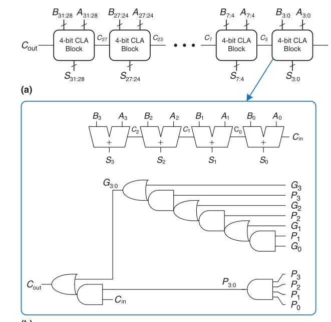
An improvement we can make to these adders are calculating the sum and product of the inputs A and B ahead of time to improve the speed of the adder.
Another way to write the equation for \(C_{out}\) is
\[C_{out} = G + PC_{in}\]Where
\[P = A + B\] \[G = AB\]From here we can define the carry out of a particular bit as
\[C_i = G_{i:j} + P_{i:j}C_j\]Where \(G_{i:j} = G_{i} + ... \ P_{j+2}(G_jP_{j+1} + G_{j+1})\)
and \(P_{i:j} = P_iP_{i-1}...P_{j-1}P_j\)
The time for the carry lookahead adder of \(N\) bits with \(k\) bit blocks is
\[t_{CLA} = t_{pg} + t_{pg\_ block} + (\frac{N}{k} - 1)t_{AND\_ OR} + kt_{FA}\]- \(t_{pg}\) is the time to find a single generate/propagate (a single AND or OR gate)
- \(t_{pg\_ block}\) is the time to find \(P_{i:j}\) and \(G_{i:j}\) for a \(k\)-bit block.
- \(t_{AND\_ OR}\) is the delay for the AND+OR block that of the last \(k\)-bit CLA adder block.
- \(t_{FA}\) is the time to compute the sum for a \(k\)-bit block
Below is an image representing a 4-bit CLA block for a 32-bit adder
Prefix Adder
The prefix adder takes the carry-lookahead adder and improves upon the design even more by giving the optimal placement of carry-lookahead components.
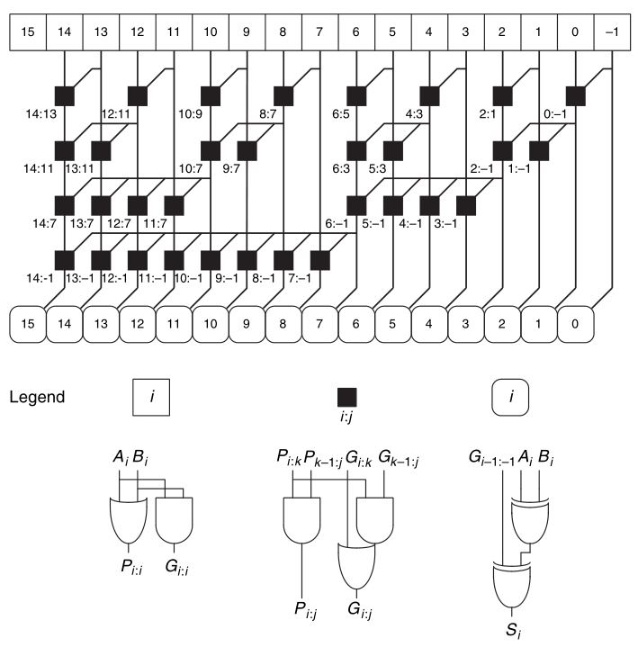
The time delay of a prefix adder is
\[t_{PA} = t_{pg} + log_2(N)t_{pg\_ prefix} + t_{XOR}\]where \(t_{pg_\_ prefix}\) is the delay of the black prefix cell.
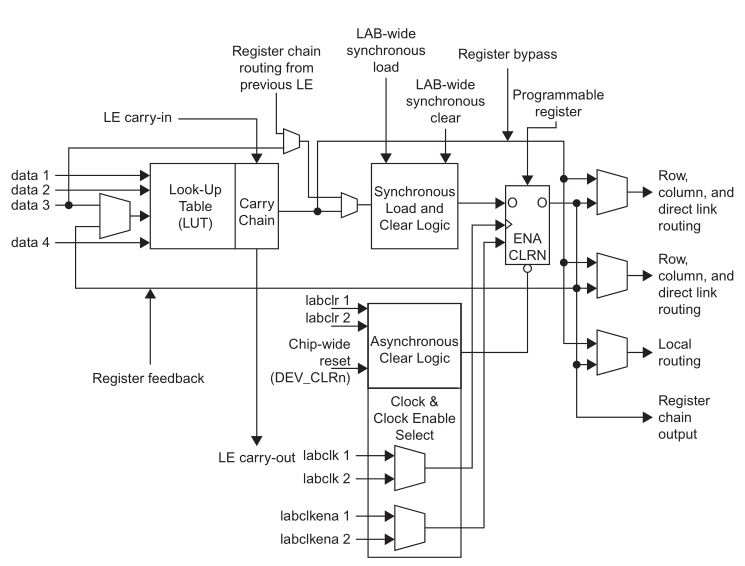
Logic Arrays (FPGA Blocks)
FPGA stands for Field programmable gate array. It is a set of logic elements which can perform a variety of functions in order to create programmable logic boards.
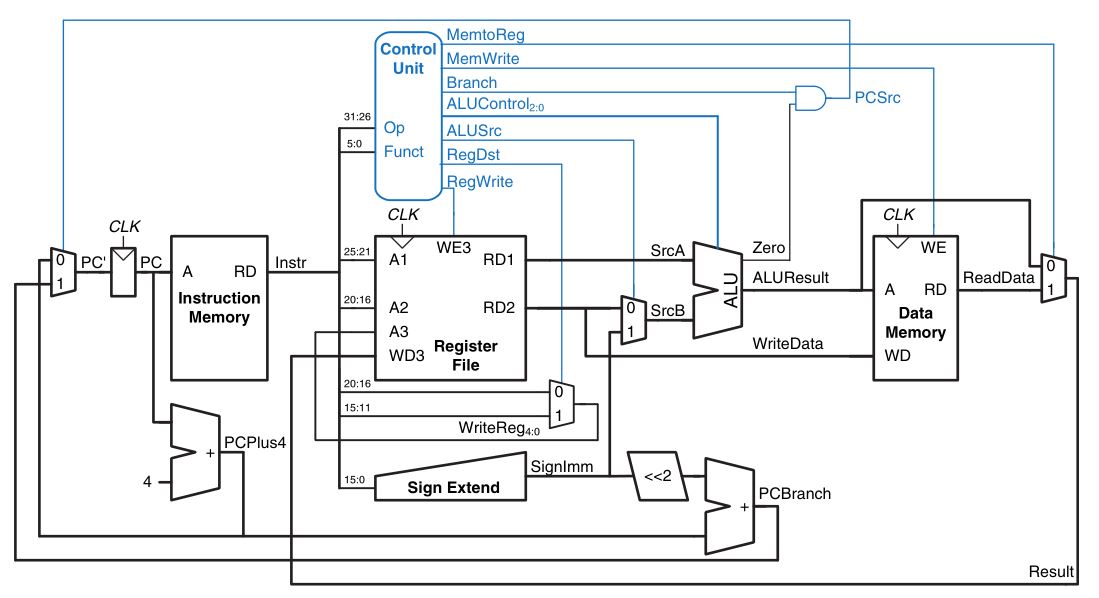
Chapter 6 - Assembly, Comp. Arch & MIPS
Instruction Types
- R Type
- op, rs, rt, rd, shamt, funct
- 6, 5, 5, 5, 5, 6 bits respectively.
- Used for register-based arithmetic instructions
- I Type
- op, rs, rt, imm
- 6, 5, 5, 16 bits respectively
- Used for arithmetic operations with up to 16 bit constants.
- Also
lw, andsw
- J Type
- op, addr
- 6, 24 bits respectively
MIPS Single Cycle Processor
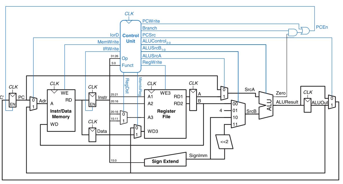
MIPS Multi-Cycle Processor